interrupt_tv

joined 4 months ago

Thank you. Diode ROMs are cool. You can see the bits! I particularly like the aesthetics of this one:

https://www.cca.org/blog/20120222-Diode-Matrix.shtml

Not sure yet. I'll post about it when I get to that part. ๐Ÿ˜

I got it as a kit from Digicool Things. Soldering and assembly by me, but the design is theirs.


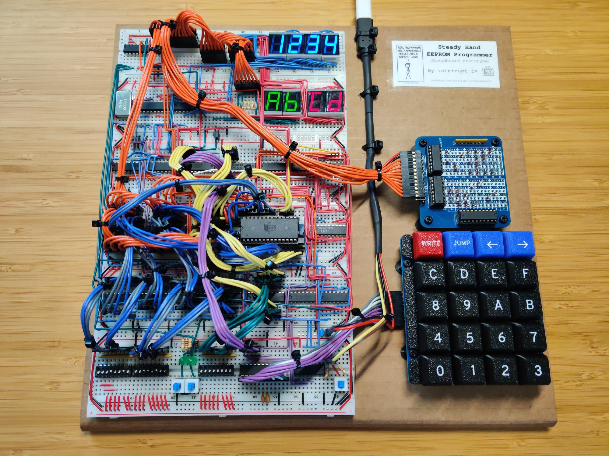
After about 6 months, my project is finally complete. It's the first significant circuit that I've designed myself, rather than just implementing someone else's design:

https://codeberg.org/interrupt_tv/steadyhand

Steady Hand is a digital circuit for programming EEPROMs by hand. It's inspired by this video by Ben Eater, where he creates a circuit for programming an EEPROM using DIP switches and jumper wires. Steady Hand is much more ergonomic than his design, though it is somewhat more complex.

While Ben Eater provides the "how" inspiration, the "why" inspiration comes from Jeremiah Orians' stage0 project, and the general concept of bootstrapping: creating a computer software environment from nothing. When building a homebrew computer, one would typically use a significantly more complex modern computer to write the homebrew computer's software to an EEPROM. I created Steady Hand as a first step towards resolving this problem.

After I'd wired everything up, I was a little afraid something would melt when I plugged it in. While the schematic is separated into smaller modules, the breadboard layout ended up being pretty monolithic. I didn't do any testing as I was assembling it, so it seemed likely there would be a mistake somewhere. No magic smoke escaped though, and it mostly worked on the first try. There were a few bugs:

  • The address display was connected backwards, with the most significant digit on the right instead of the left. Easy enough to fix, but the relevant wires were no longer the right lengths to neatly reach their connection points. This trend continued as I had to do further circuit surgeries, leaving things messier than I'd like.

  • The auto-skip function would cycle endlessly if the byte value to skip matched what was in the write registers. The write registers' output lines are connected to the EEPROM's I/O lines in order to be able to write to it. The comparator is also connected to these so that it can compare the EEPROM's output to the skip value. When it's time for the multiplexed display to show one of the write nibbles, the EEPROM's output is disabled and the write registers' output enabled. This meant that the comparator would now be comparing with the write value instead of the value read from the EEPROM, and would give the signal to skip to the next address.

    Disabling the comparator when it's getting invalid input would have required some additional logic, and at the time I didn't have any extra gates available. I solved this by using one of the display digit enable lines as the auto-skip function's clock signal, instead of having it hooked directly to the clock. This ensured that the rising edge would only occur when the comparator had a valid input.

  • After writing a byte or when auto-skipping past a large number of addresses, the EEPROM would occasionally output FF instead of the byte that was actually stored at that address. It wouldn't do this with any kind of consistency, but the FF would persist until the address was changed. I thought this was a power issue, but no combination of decoupling capacitors or pull-up resistors would make it go away. After wrestling with it for a long time, I eventually concluded that the AT28C256 just doesn't like being always enabled. Once I added proper logic to control both the output enable and chip enable lines, the problem went away.

Since I needed at least one more logic IC to solve that last bug, I decided to add a 74HC7266 quad XNOR IC. This allowed me to add a search function alongside the auto-skip function, by just using an XNOR gate to invert the comparator's output.

I used dupont cables to group related signal lines together, but I'm not sure how I feel about them now. I thought that they'd result in a cleaner layout than if I'd used several additional layers of solid core wire, but I still ended up with a rat's nest. That was likely inevitable with how densely packed the components are. If I were to redo everything, I'd probably spread them out onto more boards, group them into individual modules, and allow for more redundancy in the glue logic.

Still, I'm happy with how the project turned out overall, and that I can now move onto the next one.
[โ€“] interrupt_tv@piefed.world 2 points 1 month ago (1 children)

They're 22awg solid. Most of them are from Jameco and have PVC insulation. The bright green and dark blue wires are from Ben Eater's World's Worst Video Card kit, and have what feels like silicone insulation.

[โ€“] interrupt_tv@piefed.world 1 points 2 months ago

With extra USB cables as a garnish. Very nice.

[โ€“] interrupt_tv@piefed.world 1 points 2 months ago

I reorganized my breadboard computer. What happened next will shock and amaze you!

[โ€“] interrupt_tv@piefed.world 4 points 2 months ago

It's not too difficult to learn. Ben Eater is really good at teaching this stuff. He guides you through everything in small steps that are easy to understand: https://www.youtube.com/watch?v=LnzuMJLZRdU

[โ€“] interrupt_tv@piefed.world 4 points 2 months ago

Thank you. I've got the PCB design and assembly instructions here if you want to make your own: https://codeberg.org/interrupt_tv/alpz-bb

Not sure exactly how long it took. I worked on it off and on over the span of a few days.

[โ€“] interrupt_tv@piefed.world 4 points 2 months ago

Definitely a great resource. I've got it bookmarked to read more of later. From the address decoding chapter, I can now better appreciate Ben's weird memory layout that leaves half of the RAM inaccessible. It allows you to hook up a ton of peripherals and use the individual address lines to select them. You can even select multiple devices to write to simultaneously, depending on which part of the address space you access.


My main project has been paused while I waited for a shipment of components. Who knew I would need an XNOR gate IC?

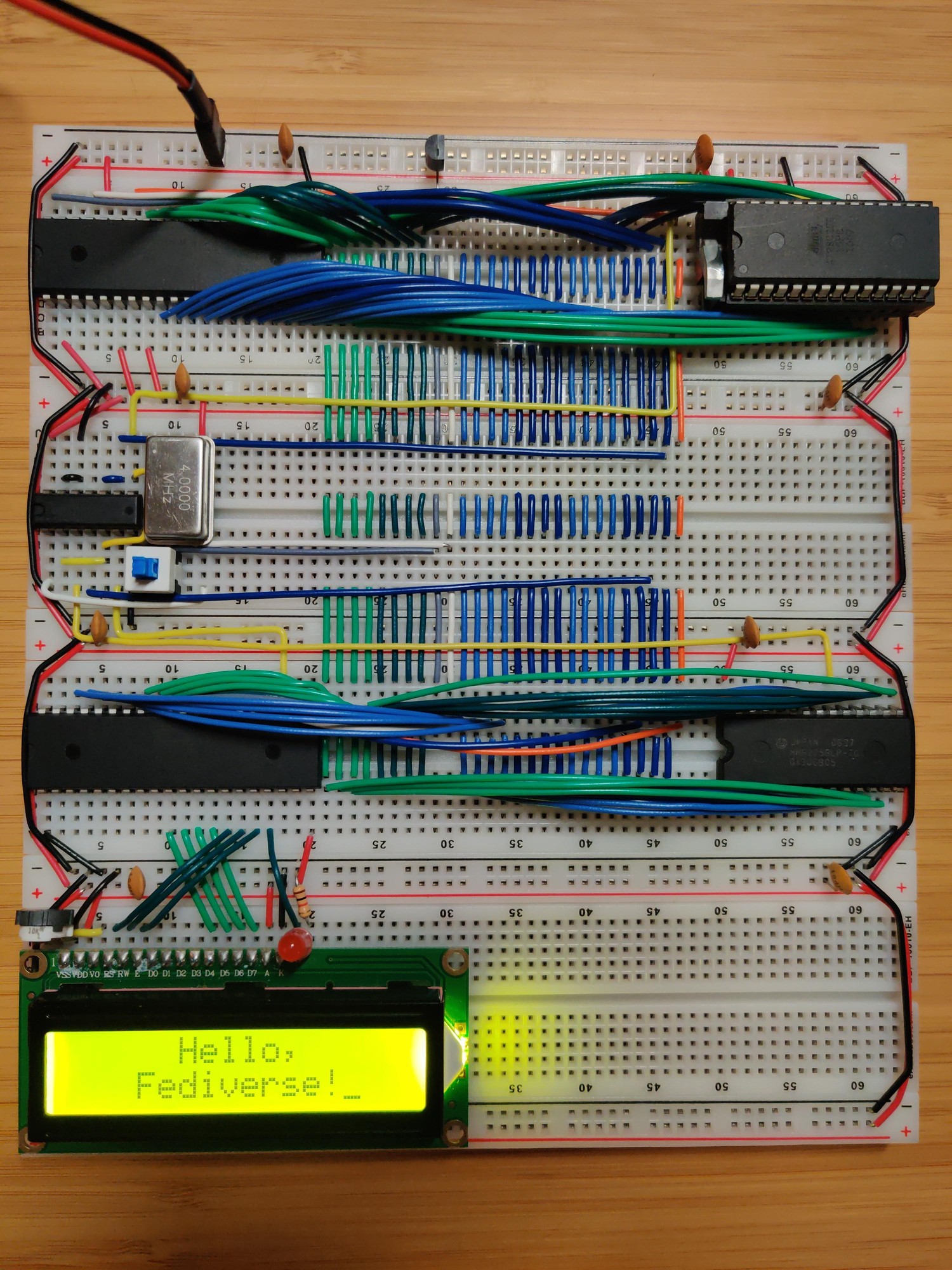
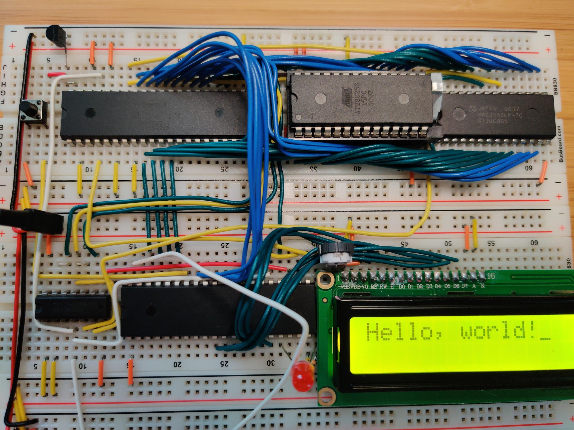
In the meantime I switched back to working through Ben Eater's videos on the 6502. I'm up to the ones on implementing the PS/2 keyboard interface. Before getting too far into it, I decided it was finally time to clean up the layout of the computer's components. Ben's layout, while compact, is also pretty messy. The address and data buses wind all over the place, making them difficult to understand and access for diagnostics or expansion. Also when I first built it I hadn't bothered to take any power rails off of the boards before connecting them together, so my power rails were doubled up:

2qmhr9dONxZwnFA.jpg

Inspired by some layouts that I'd seen on r/beneater, I went with a layout that has all the bus lines running vertically through the center of each board. Components are placed on the sides and connect to the bus lines instead of directly to each other. There are 27 bus lines:

  • 8 data lines (light green for the low nibble, dark green for high)
  • Reset (gray)
  • Clock (white)
  • 16 address lines (alternating light and dark blue for each nibble)
  • CPU read/write signal (orange)

There's just enough room on the left side for the DIP40 ICs. The DIP28s go on the right, with a few columns to spare. Since the data bus starts at column 21, it aligns nicely with the numeric labels on the breadboard. The 1st data line is at column 21, 2nd line is at 22, 3rd at 23, and so on. I put the reset and clock lines in between the data and address busses in order to maintain this pattern for the address lines: 1st at 31, up to 16th at 46. I guess I could have gotten 0-based indexing instead of 1-based if I had put the DIP40s on the right side, but the 6502 really wants to be on the left side due to its pin layout.

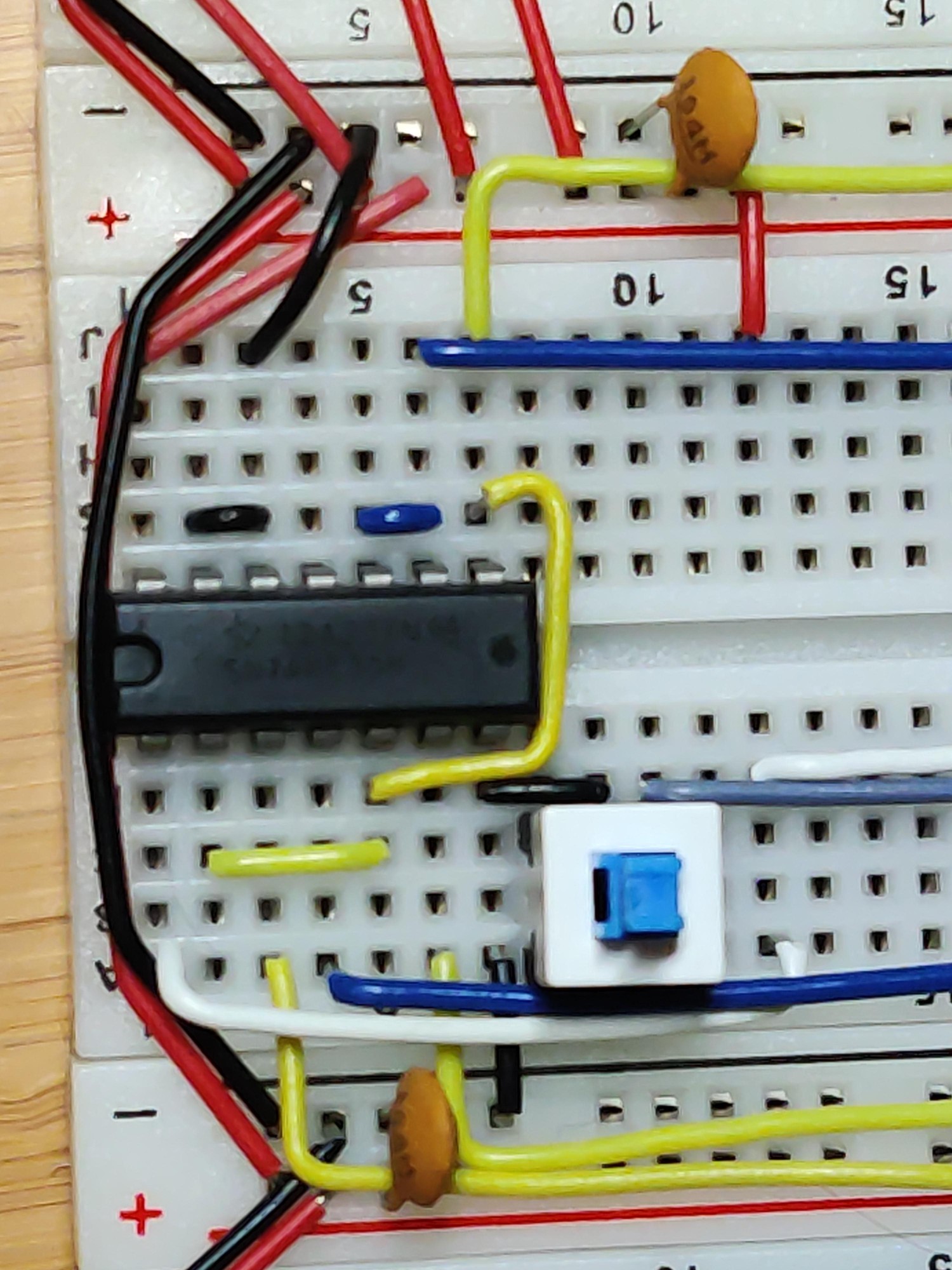
I also did some creative wiring in order to fit the reset button below the oscillator so that it wouldn't take up any extra real estate:

A681824S5Law1RY.jpg

The center pins of the button share a column with the GND pin of the oscillator. The left pins are in the unusable space between the oscillator and the NAND IC. The right pins are in an otherwise unused column that runs underneath the oscillator. Since the reset button doesn't take up any extra space, there's room for an additional DIP14 next to the oscillator, and another two DIP14s or DIP16s to the right of the bus on that board.

[โ€“] interrupt_tv@piefed.world 1 points 2 months ago

Ah, sorry, I could have been more clear there. It can do arbitrary mappings between input values and output values. So for each possible 4-bit value, you can pick a different 8-bit value to be output.

For my case, I'm working with a 7-segment LED display, like the display on a microwave. It's got 7 LEDs arranged to display a number, plus an 8th LED for a decimal point. Like this:


|   |

|   |

.

if the ROM is getting 0000 for its input, it should light up all segments of the 7-segment display except for the horizontal one in the center, to display a zero. Then for the 0001 input, it should light up the two vertical segments on the right, leaving the rest dark, to display a one. And so on. Each output bit goes to a particular segment of the display.

To relate it more directly to programming, it's like having a 16 byte array. The input gives the array index that you want to access, and the output gives whatever byte is at that index.

[โ€“] interrupt_tv@piefed.world 2 points 2 months ago (2 children)

Oh, that's cool. I hadn't heard of slimevr before.

My use case for the diode ROM board is to take 4 binary input bits (16 possible combinations) and translate them into what segments of a 7-segment LED display should be lit or unlit, in order to display the corresponding hexadecimal digit (0-9, A-F). Like so:

Diode ROM in use

It could be used for any other case where you need to convert a 4-bit input into 16 possible 8-bit outputs. In theory you could use them in multiples for more address space, but I forgot to include an enable pin on the board to allow for that. Something to add to the next version.

[โ€“] interrupt_tv@piefed.world 5 points 2 months ago (4 children)

Not programming per se, but I've been working on some electronics projects. If you check my profile, there's two PCB designs that I've posted. They're fairly simple, but I'm working on a larger project that I should be posting relatively soon. Currently I'm just waiting on a shipment of parts, because I didn't realize I would need XNOR gates.


Do you need 16 bytes of ROM that you can program with a soldering iron? Well, you're in luck!

I'm working on a larger project that I'll hopefully be sharing here soon, and needed something to display hexadecimal digits on a 7-segment LED display. The non-obsolete ICs that I found could only do binary coded decimal, but I need to be able to display A-F as well. An EEPROM truth table can be used for this, but I also wanted to avoid any programmable ICs. I decided to take an old-school approach and create a diode ROM board.

Diode ROM parts

Diode ROM assembled

Diode ROM in use


I've been working on Ben Eater's breadboard 6502 computer project for a little while. The pins on the EEPROM sometimes get bent when I pry it out of the breadboard to reprogram it. I was afraid that they'd break eventually, so I looked into getting a Zero Insertion Force (ZIF) socket to put on the board, which should be gentler on the EEPROM's pins. Ran into a few problems though:

  • The pins on ZIF sockets are too short to seat properly on a breadboard. They're designed to be soldered into a printed circuit board.
  • I found a few designs for adapter PCBs that allow a ZIF socket to be used on a breadboard. They're all sized for the common green ZIF sockets, which take up a lot of extra space compared to the chip that they hold.
  • Aries Electronics makes low-profile ZIF sockets that are very compact, but I couldn't find any adapters designed for them.

I eventually decided to solve that last one myself, and I figured I'd share the design in case anyone else might find it useful:

view more: next โ€บ